Re-Exposure is an occasional Motherboard feature where we look back on delightful old tech photos from wire service archives.
“It looks like a three-dimensional skyline. You can get totally lost in it.”
Last year, photographer Christoph Morlinghaus gained notice in Wired for a project of his that involved taking very high-resolution shots of microprocessors throughout computing history. Some of the chips he shot, like the Cyril GXm, were underpowered minor players in computing history. But they still look interesting.
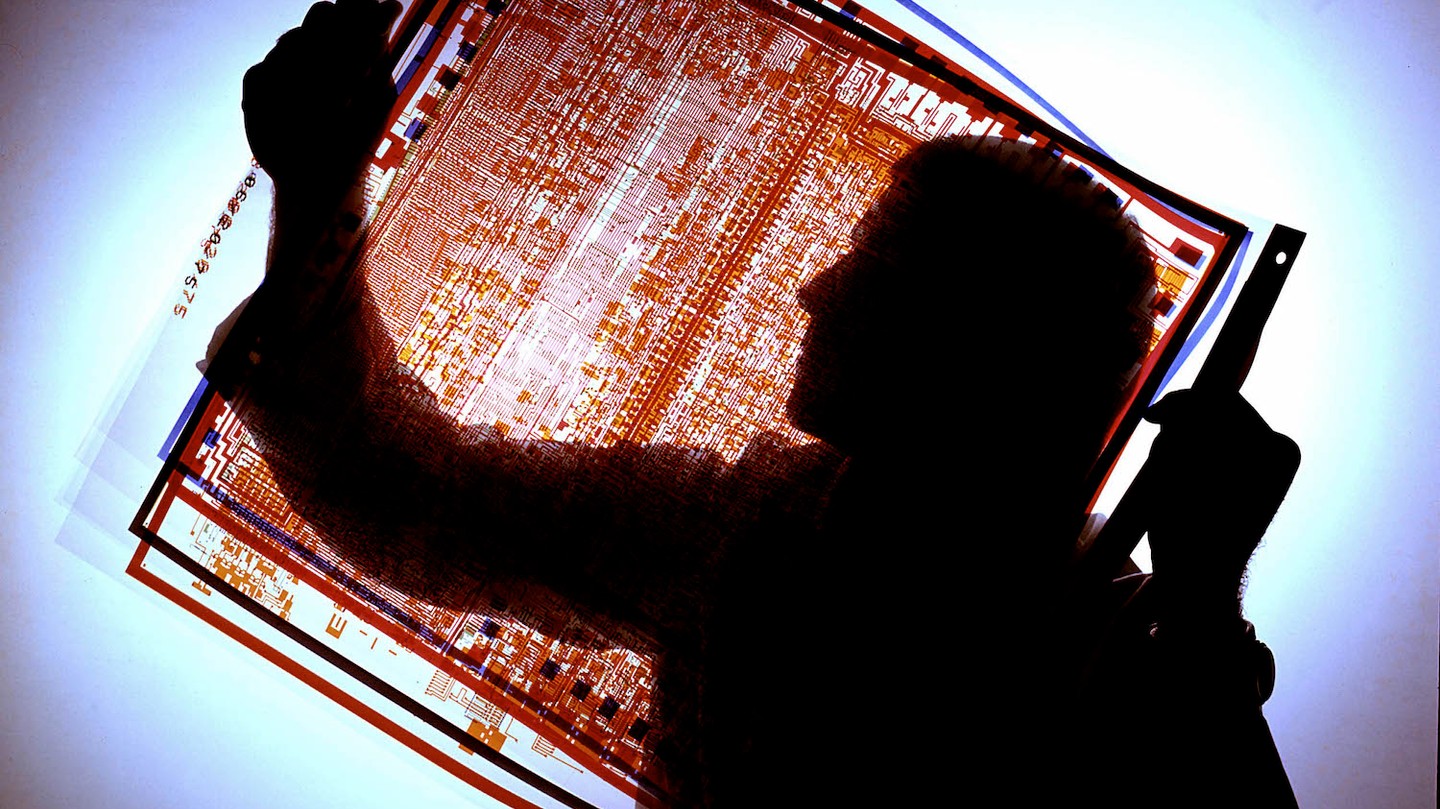
So how do they get these impossibly complex designs into the processors? That leads us to the photo above, featuring a Motorola engineer in the 1970s, taking a close look at the drawn transistors of a computer chip. These sheets, all color-coded, would soon be printed onto a piece of silicon, giving a tightly-wound processor more computing ability than one could ever get from a printed circuit board on its own.
A major innovation came about in the computing space roughly a decade prior, when it was realized that transistors could be drawn into complex integrated circuits. Those circuits, tightly packed and incredibly detailed, are printed at tiny sizes onto silicon wafers. This process, invented by Texas Instruments researcher Jack Kilby, got around a major problem at the time—the “tyranny of numbers,” or the idea that you can only fit so many transistors into a certain amount of space. By making the transistors tiny, you can fit a whole lot more, clearly. (Though it makes the chips more susceptible to dust, hence the existence of “clean rooms.”)
But what about putting them on the chip? That involves a process called photolithography, which shrinks the circuit designs to a tiny scale and embeds them onto purified silicon. This YouTube clip, featuring UK-based Microsoft Research director Christopher Bishop, does a good job of explaining the photolithography process. Initially, Bishop asks a young girl to write her initials on a grain of rice, which she clearly can’t do. Then he hands her a clear sheet of paper, has her put her initials on that, then uses a combination of light and lenses to display a picture of those initials on a grain of rice. When printing on silicon, chemicals are added to the process, effectively “printing” the design to the wafer.
It’s kind of like microfilm, except on steroids—and it’s the basis behind pretty much every computing device you use.
A Motorola engineer looking at masks for chip engraving in 1975. Image: Henry Groskinsky/The LIFE Images Collection/Getty Images
 Techosta Where Tech Starts From
